Subscribe by email

Power Supply circuits diagram electronics projects

Power Supply circuits diagram electronics projects: battery chargers, switching power supply , ac power supply, dc dc converters, power inverter, converters and power adapters .

LNB power supply

Using the LNBH23L monolithic voltage regulator and interface IC can be designed a very simple high efficiency LNB power supply .
LNBH23L monolithic voltage regulator is specifically designed to provide the 13 / 18 V power supply and the 22 kHz tone signalling to the LNB down-converter in the antenna dish or to the multi-switch box. In this LNB power supply circuit offers a complete solution with extremely low component count, low power dissipation together with simple design and I²C standard interfacing.

The design for this LNB power supply is very simple and require few external components . LNBH23L voltage regulator has a built-in DC-DC step-up converter that, from a single source from 8 V to 15 V, generates the voltages (VUP) that let the linear post-regulator to work at a minimum dissipated power of 0.55 W typ. @ 500 mA load. An under voltage lockout circuit will disable the whole circuit when the supplied VCC drops below a fixed threshold (6.7 V typically).

Some features of this power supply circuit diagram are : auxiliary modulation input , accurate built-in 22 kHz tone generator suits ,overload and over-temperature internal protections with I²C diagnostic bits , LNB short circuit dynamic protection.
LNBH23L LNB power supply circuit diagram

5 volt power supply using LNK584DG IC

A very simple high efficiency power supply electronic project can be designed using the LNK584DG circuit designed by Power Integrations . The LNK584DG circuit is a very nice IC from LinkZero-AX, that helps you to design a very simple high efficiency switching power supply circuit using few external electronic components . This switching power supply circuit diagram is a typical non-isolated 5 V, 300 mA output auxiliary power supply using LinkZero-AX.

This circuit is typical of auxiliary supplies in white goods where isolation is often not required. AC input differential filtering is accomplished by the π filter formed by C1, C2 and L3. The proprietary frequency jitter feature of the LinkZero-AX eliminates the need for any Y capacitor or common-mode inductor. Wire-wound resistor RF1 is a fusible, flame proof resistor which is used as a fuse as well as to limit inrush current. Wire wound types are recommended for designs that operate >132 VAC to withstand the instantaneous power dissipated when AC is first applied.

The output voltage is directly sensed through feedback resistors R3 and R9, and regulated by LinkZero-AX (U1) via the FEEDBACK pin. Capacitor C7 provides high frequency filtering on the FEEDBACK pin to filter noise and to avoid switching cycle pulse bunching. The controller in U1 receives feedback from the output through feedback resistors R9 and R3.

Based on that feedback, it enables or disables the switching of its integrated MOSFET to maintain output regulation. Switching cycles are skipped once the FEEDBACK pin threshold voltage (1.70 V) is exceeded. When the voltage on the FEEDBACK pin falls below the disable threshold (1.70 V), switching cycles are re-enabled. By adjusting the ratio of enabled to disabled switching cycles the output voltage is regulated. At increased loads, beyond the output peak power point, where all switching cycles are enabled, the FEEDBACK pin voltage begins to reduce as the power supply output voltage falls. Under this condition the switching frequency is also reduced to limit the maximum output overload power.

When the FEEDBACK pin voltage drops below the auto-restart threshold (typically 0.9 V on the FEEDBACK pin), the power supply enters the auto-restart mode. In this mode, the power supply will turn off for approximately 1.2 s and then turn back on for approximately 170 ms. The auto-restart function reduces the average output current during an output short-circuit condition.
As you can see in the circuit diagram , this power supply circuit is very simple an can be powered using a wide range input voltage from 85 up to 265 VAC .
5 volt switching power supply circuit schematic using LNK584DG IC

Tube T8 power supply

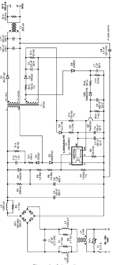
A simple led driver for T8 lamps can be designed using the LNK406EG circuit designed by Power Integrations . This Led driver circuit will drive can be used for high power LEDs pplications and it can drive a nominal LED string voltage of 50 V at 0.3 A from an input voltage range of 90 VAC to 265 VAC.
The topology used is an isolated flyback operating in continuous conduction mode.
Output current regulation is sensed entirely from the primary side eliminating the need for secondary side feedback components. The internal controller adjusts the MOSFET duty cycle to maintain a sinusoidal input current and therefore high power factor and low harmonic currents.

Fuse F1 provides protection from catastrophic component failure while RV1 (MOV)
provides a clamp to limit the maximum component voltage stress during differential line surges.
Diode bridge BR1 rectifies the AC line voltage with capacitor C2 providing a low impedance path (decoupling) for the primary switching current. A low value of capacitance (sum of C1, C2 and C3) is necessary to maintain a power factor of greater than 0.9.

EMI filtering is provided by inductors L1, L2, L3 and L4, C1 and Y1 safety rated C8.
Diode D1 and C3 detect the peak AC line voltage. This voltage is converted to a current which is fed into the V pin via R5, R6 and R7. This current is also used by the device to set the input over/under voltage protection thresholds. The V pin current and the FB pin current are used internally to control the average output LED current. The non-dimming mode of LinkSwitch was selected via a 24.9 k resistor on the R pin One end of the flyback transformer is connected to the DC bus while the other is driven by the integrated 725 V power MOSFET within U1. During the power MOSFET on time the primary current ramps up, storing energy in the transformer. This energy is transferred to the secondary when the power MOSFET turns off. An EER25 core was selected for low profile and used a triple insulated secondary winding with flying leads to meet safety spacing requirements.
Diode D3 is necessary to prevent reverse current from flowing through the LinkSwitch-PH device .

Diode D5, C5, R13 and R11 create a supply from the bias winding on the transformer.
This voltage supplies the operating current into the BYPASS pin of U1 through D4 and R9. Capacitor C4 provides local decoupling for the BYPASS pin. It is also used during startup, being charged to ~6 V from an internal high-voltage current source tied to the device DRAIN pin. Diode D6, R16, C7, R14, VR2, C6, R12, and Q1 provide an open load overvoltage
protection function.

A current proportional to the output voltage is fed into the FEEDBACK pin through R10 from the primary bias supply. This current together with the V pin current is used to maintain the average output current to be constant with changes in input and output voltage.
Diode D7 rectifies the secondary winding while capacitors C9 and C10 filter the output. A small pre-load is provided by R15 which limits the output voltage under no-load conditions and inductor L5 is used to reduce radiated EMI.
 t8 tube driver schematic circuit using LNK406EG IC

Pages

Subscribe to RSS - Power Supply