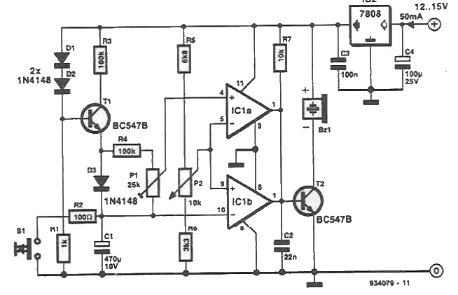
Timing circuit with buzzer and ao
This timing circuit is realized using operational amplifiers and transistors. Element determining the timing of this circuit is the capacitor C1, which is loaded by a current source made by T1.
With values given in the diagram, the time ranges is between 1 and 10 minutes.
Ramp and reference voltage are compared with IC1a and IC1b, both with collector outputs. Ignoring for the moment ICla, IClb's output transistor will be blocked as long as fixed voltage is higher than the potential of C1. If this potential is higher than the reference voltage, the transistor output of lead and T2 IClb locks.
A buzzer output activates after a period of time has elapsed from the start, and the second output disables the buzzer after a period somewhat higher leakage from power. Thus, the buzzer sounds only during the brief overlap of the two periods. During this overlap is fixed with P1. Interval before activating buzzer is set to P2, and timing starts when pressing S1.


Add new comment